
Semiconductor manufacturing
Wafer Handling Robot for Semiconductor
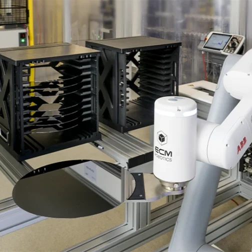
Looking to make the transfer of your wafers more reliable, from R&D to full-scale production? ECM Robotics designs and integrates wafer handling robots for you: substrate transfer, cassette management, alignment, and traceability for both lots and individual wafers. These systems draw on our expertise in robotic solutions, combining deep knowledge of semiconductor processes with industrial robotics integration.
Over 20 Years of Expertise Serving Your Production Lines
For over 20 years, we’ve automated your cleanroom production lines for semiconductor and photovoltaic manufacturing. Our turnkey robotic systems and gripping solutions are built to transport your sensitive substrates at high throughput, without compromising the quality or safety of your process. This hands-on expertise lets us adapt immediately to your constraints: cleanroom class requirements, substrate fragility, throughput targets, and factory compliance standards with no learning curve for your teams. We know your needs vary by industry. If you produce semiconductor wafers, your priority is precision: tight tolerances, high-value substrates, zero defects.
If you produce for photovoltaics, your priority is speed, without compromising breakage rates or line uptime keeping pace with higher-volume, lower-margin production. Either way, we design transfer systems calibrated to your exact profile, built on the same proven integration platform for faster, more reliable deployment. Wafer handling is just one aspect of our expertise in robotic integration. We apply the same precision engineering approach to other high-value industrial processes: robotic heat treat system, battery pack assembly, and robotic welding.
The Precision Your Fragile,
High-Value Substrates Demand.
Whatever your wafers, your integration meets three requirements:
- Precision and repeatability: across all substrate types and sizes, to limit your risk of edge damage and breakage
- Transfer speed: without loss of placement accuracy
- Adaptive design: from your low-cadence R&D station to your high-throughput production line, on the same integration base
From R&D to Production:
One Integration Expertise.
For Your R&D Applications: Piece-by-Piece, Multi-Format Handling
For your R&D, we integrate piece-by-piece handling systems that support multiple substrate formats within the same setup. Your teams can test across formats without redesigning their equipment for every new project.
For Your Production: Large-Scale Cassette Loading
For your production, our cassette management solutions are built for high-volume lines, maintaining processing precision and production cadence.
Our Core Capabilities
Serving Your Semiconductor Automation.
Our wafer processing integrations are built from the following functional blocks:
Wafer Gripping and Transport
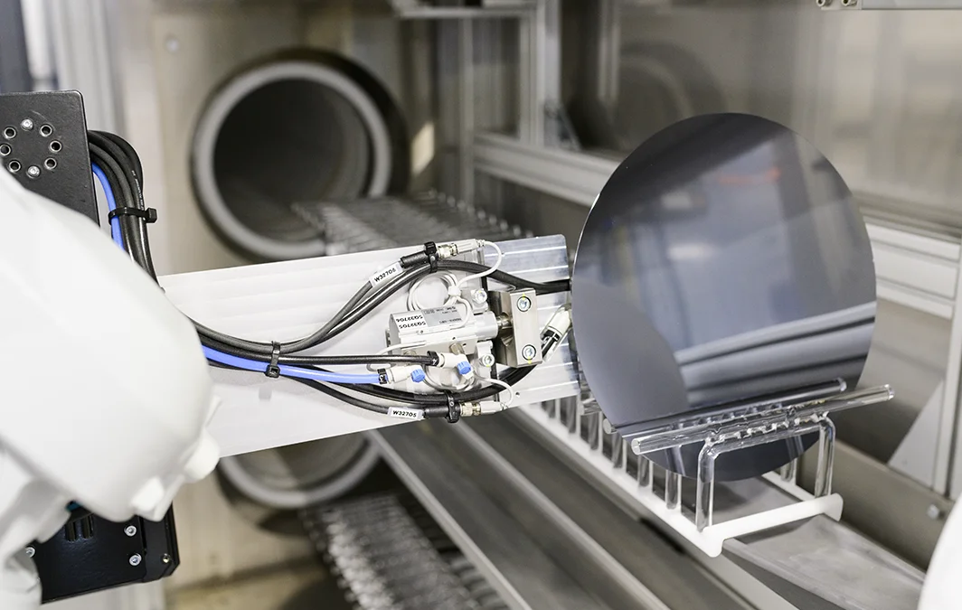
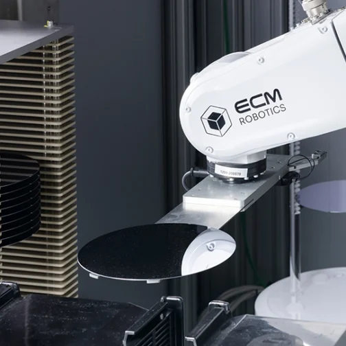
Precise, fast gripping of your wafers, whatever their size or fragility level — to minimize contact stress and reduce your risk of breakage.
Cassette Mapping
Automated checks confirm wafer presence, position, and slot occupancy in your cassettes before handling begins, reducing your risk of upstream processing errors.
Wafer Aligner
Integrated alignment stations correct your wafers’ orientation (notch or flat) before the substrate continues on its path, ensuring consistent positioning at every stage.
Wafer Marking Reading (Datamatrix / OCR)
Automated reading of your wafers’ ID marks ensures traceability and quality control, linking each substrate to its process history from its first handling step.
Buffer Management
Management of intermediate storage for your wafers between process steps, keeping your production flow running when your downstream equipment operates at different cadences.
Load Reshuffling
Automated reordering of your wafer processing sequence, adapting production order to your changing priorities without manual intervention.
Wafer-to-Wafer Tracking
Individual tracking of each wafer throughout its production journey, supporting traceability, yield analysis, and root-cause investigation.
Factory Host Communication (SECS/GEM)
Continuous communication with your factory host systems via the SECS/GEM protocol, letting your equipment exchange status, data, and alerts with your MES infrastructure.
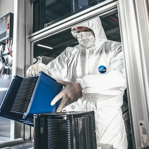
Cleanroom and Collaborative
Environment Integration.
We integrate your wafer handling solutions in both enclosed cleanroom environments and collaborative environments, where the robot works directly alongside your operators. Cleanroom integration meets your contamination control requirements; collaborative integration meets your safety and ergonomics requirements on a shared workstation.
What Gains Can You Expect
from Wafer Handling Robotics?.
Robotic wafer processing integration improves several measurable outcomes for your production:
- Fewer losses with high-precision gripping solutions tailored to your substrates
- Reduced contamination risk with systems that meet cleanroom requirements
- Improved safety and ergonomics on your collaborative workstations
- Full traceability through code reading and built-in quality control
- Scale-up potential, from a single R&D cell to a full production line
Talk to Our Specialists
ECM Robotics supports your automated wafer production projects, from R&D through production, including upgrades to your existing cleanroom cells and the integration of collaborative solutions.